EIE VLSI Lab 5 - VGA Controller (Compiled & working on Quartus v20.1)
EIE VLSI Lab 5 - VGA Controller
(To be compiled on Quartus v20.1) Using Verilog

Datasheet file of Video DAC: https://www.analog.com/media/en/technical-documentation/data-sheets/adv7123.pdf
You could understand the principle from the above website of eewiki.


(extracted diagram from the user manual of DE1-SoC)
Pin assignment of the I/Os to connect to control the video DAC chip:

Files:
This part will use remote-desktop to access the hardware in the lab CF504 inside the PolyU campus. Each PC has been done with the first four of the following (by EIE technical staff):
1. Connect the FPGA board to the power, the JTAG USB Blaster cable to PC.
2. Power the FPGA on.
3. Connect the VGA output of the board to another monitor.
4. Connect a camera to the PC for remote viewing.
5. Zip and upload your local project folder into a zip file into e.g. PolyU One Drive / Google Drive.
6. Login the remote desktop using UDS: https://puuds.polyu.edu.hk/uds/page/login (PolyU net ID)
7. Choose CF502.
8. Check your hardware in the remote PC. Find the app “Camera” and you can see the board DE1-SoC. You can also check the driver in “Device Manager” (under “JTAG cable”).


9. Download your project file from e.g. One Drive to a local folder, e.g. c:\QuartusProjects\
10. Open your project in Quartus v20.1 and the programmer (double-click) in the remote PC:

· Click on "Hardware Setup" button to check and select DE-SoC[USB-1] FPGA


· Select 5CSEMA5

You should see two chips: SOCVHPS and SCSEMA5 (if not, click “Auto Detect” again).
Right click on 5CSEMA5 device à change file à select the file /output_files/VGA1_V.sof
(Note: make sure that the 2nd device 5CSEMA5 is selected for this part)

Click on Auto-detect if the start button is not enabled à Start (to program)

The FPGA should have been successfully programmed.
The FPGA should have been successfully programmed as shown above. The hardware programming test part is finished. You can continue to try to do the simulation and modifications on your local PC.
Remember to sign out the remote desktop (Do NOT just close the browser)

(my installation folder is "c:\intelFPGA_lite\20.1" and you need to change it if it is different)
Then locate the compiled test bench (tb_VGA1_V) under the work library (double-click it):


Select the signals and add them to the waveforms:

vsim work.tb_VGA1_Vadd wave -position insertpoint \sim:/tb_VGA1_V/i1/CLK \sim:/tb_VGA1_V/i1/RST_N \sim:/tb_VGA1_V/i1/VCLK \sim:/tb_VGA1_V/i1/VGA_SYNC \sim:/tb_VGA1_V/i1/VSYNC \sim:/tb_VGA1_V/i1/HSYNC \sim:/tb_VGA1_V/i1/BLANK \sim:/tb_VGA1_V/i1/VGA_R \sim:/tb_VGA1_V/i1/VGA_G \sim:/tb_VGA1_V/i1/VGA_B \sim:/tb_VGA1_V/i1/clk_div2 \sim:/tb_VGA1_V/i1/hPos \sim:/tb_VGA1_V/i1/vPos \sim:/tb_VGA1_V/i1/hs \sim:/tb_VGA1_V/i1/vs \sim:/tb_VGA1_V/i1/de \sim:/tb_VGA1_V/i1/pll_clkout \sim:/tb_VGA1_V/i1/pll_locked \sim:/tb_VGA1_V/i1/SYNCrun 5000000


Then the waveform window shows:

The horizontal position counter (hPos) increases at the rising edge of the pixel clock (VCLK) and the vertical position counter (vPos) increases when the horizontal position counter overflows:


// ----- EIE511 Project Sample - VGA Controller //
module VGA1_V (CLK, RSTN, VGA_CLK, VGA_VS, VGA_HS, VGA_BLANK_N, VGA_SYNC_N, VGA_R, VGA_G, VGA_B);
input CLK; // System Clock Input (FPGA)
input RSTN; // System Reset Signal (FPGA active low)
output VGA_CLK; // VGA Pixel Clock
output VGA_SYNC_N; // VGA Sync Signal
output reg VGA_VS; // VGA Vertical Sync (vsync) Signal
output reg VGA_HS; // VGA Horizontal Sync (hsync) Signal
output reg VGA_BLANK_N; // VGA Blank Input
output [7:0] VGA_R; // VGA 8-bit Red Input
output [7:0] VGA_G; // VGA 8-bit Green Input
output [7:0] VGA_B; // VGA 8-bit Blue Input
parameter HD = 16'd1024; // Horizontal Resolution (640)
parameter HFP = 16'd24; // Right border (front porch)
parameter HSP = 16'd136; // Sync Pulse (Re-trace)
parameter HBP = 16'd160; // Left boarder (back porch)
parameter HPOS_MAX = HD + HFP + HSP + HBP - 1; // Calculation of H-Position Max.
parameter VD = 16'd768; // Vertical Display (480)
parameter VFP = 16'd3; // Right border (front porch)
parameter VSP = 16'd6; // Sync pulse (Retrace)
parameter VBP = 16'd29; // Left boarder (back porch)
parameter VPOS_MAX = VD + VFP + VSP + VBP - 1; // Calculation of V-Position Max.
// reg clk_div2 = 0; // Internal Register for Divide-by-2 Clock
wire pixel_clk;
reg [15:0] hPos = 0; // Register for current Horizontal Position Storage
reg [15:0] vPos = 0; // Register for current Vertical Position Storage
reg hs = 0; // register for hsync generation (account for pixel data delay)
reg vs = 0; // register for vsync generation (account for pixel data delay)
reg de = 0; // register to indicate current position is in drawing area or not
// outputs
assign VGA_SYNC_N = 0;
assign VGA_CLK = pixel_clk; //clk_div2;
//assign pixel_clk = clk_div2;
/* // PLL Instantiation */
PLL PLL_inst
(
.refclk(CLK) , // input refclk_sig
.rst(~RSTN) , // input rst_sig
.outclk_0(pixel_clk) // output outclk_0_sig
// .locked(pll_locked) // output locked_sig
);
// Clock Divided by 2
//always @(posedge CLK) clk_div2 = ~clk_div2;
// Horizontal_position_counter (clk_div2, RSTN)
always @(posedge pixel_clk, negedge RSTN) begin
if (RSTN == 0)
hPos <= 0;
else if (pixel_clk == 1)
//hPos <= (hPos == (HD + HFP + HSP + HBP - 1)) ? 0 : (hPos + 1);
if (hPos == HPOS_MAX)
hPos <= 0;
else
hPos <= hPos + 1;
end
// Vertical_position_counter:process(pixel_clk, RSTN)
always @(posedge pixel_clk, negedge RSTN) begin
if(RSTN == 0)
vPos <= 0;
else if (pixel_clk == 1)
if (hPos == HPOS_MAX)
if (vPos == VPOS_MAX)
vPos <= 0;
else
vPos <= vPos + 1;
end
//Horizontal_Synchronisation:process(pixel_clk, RSTN)
always @(posedge pixel_clk, negedge RSTN) begin
if(RSTN == 0) begin
hs <= 1;
VGA_HS <= 1;
end
else if (pixel_clk == 1) begin
if((hPos >= (HD + HFP)) && (hPos < (HD + HFP + HSP)))
hs <= 0;
else
hs <= 1;
end
VGA_HS <= hs; //delay one clock to account for pixel data delay
end
//Vertical_Synchronisation:process(pixel_clk, RSTN)
always @(posedge pixel_clk, negedge RSTN) begin
if(RSTN == 0) begin
vs <= 1;
VGA_VS <= 1;
end
else if (pixel_clk == 1) begin
if((vPos >= (VD + VFP)) && (vPos < (VD + VFP + VSP)))
vs <= 0;
else
vs <= 1;
end
VGA_VS <= vs; //delay one clock to account for pixel data delay
end
//video_on:process(pixel_clk, RSTN)
always @(posedge pixel_clk, negedge RSTN) begin
if(RSTN == 0) begin
de <= 0;
VGA_BLANK_N <= 0;
end
else if (pixel_clk == 1) begin
if ((hPos < HD) && (vPos < VD))
de <= 1;
else
de <= 0;
end
VGA_BLANK_N <= de; //delay one clock to align with pixel data
end
//module for drawing horizontal colorbar:process(pixel_clk, RSTN)
draw_colorbar_v #(.HD(HD), .VD(VD)) inst_draw (
.CLK(pixel_clk),
.RSTN(RSTN),
.R(VGA_R),
.G(VGA_G),
.B(VGA_B),
.de(de),
.hPos(hPos),
.vPos(vPos)
);
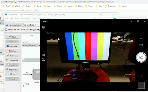
5) Outcomes on the VGA monitor:


PolyU EIE511


Thank for sharing blog read more Best ai tools in 2025
回覆刪除