Laboratory Objectives
The objectives of this laboratory are:
l Synthesize designs targeting a particular prototyping board
l Download a design to the FPGA prototyping board and have a fully functional design
l Understand the use constraint files
l Learn how to interface with the prototyping board through switches and buttons.
Introduction
The following design will output the 4 MSB of a 32-bit counter to 4 LEDs of the DE1-SoC prototyping board. By changing switch 8 of the board it should count UP or DOWN.
Terasic DE1-SoC Board
The Terasic DE1-SoC prototyping board contains a single Cyclone V FPGA connected to a serious or peripherals and interconnects in order to communicate with other devices.
Terasic's DE1-SoC board contains the following major parts:
1) FPGA:
l Cyclone V SoC 5CSEMA5F31C6 Device
l Dual-core ARM Cortex-A9 (HPS)
l 85K Programmable Logic Elements
l 4,450 Kbits embedded memory
l 6 Fractional PLLs
l 2 Hard Memory Controller
2) Switches:
l 4 User Keys (FPGA x4)
l 10 User switches (FPGA x10)
l 11 User LEDs (FPGA x10 ; HPS x 1)
l 2 HPS Reset Buttons (HPS_RST_n and HPS_WARM_RST_n)
l Six 7-segment displays
3) Memories:
l 64MB (32Mx16) SDRAM on FPGA
l 1GB (2x256Mx16) DDR3 SDRAM on HPS
l Micro SD Card Socket on HPS
4) Communications:
l Two Port USB 2.0 Host (ULPI interface with USB type A connector)
l USB to UART (micro USB type B connector)
l 10/100/1000 Ethernet
l PS/2 mouse/keyboard
l IR Emitter/Receiver
More information can be found at the manufacturers board web page at: Terasic - DE Boards - Cyclone - DE1-SoC Board
FPGA implementation of LED Counter
Open Quartus Prime
(Note: The tool may require you to choose either to purchase a license or use lite edition. Using Lite Edition is adaquate)
Verilog codes of LED Counter:
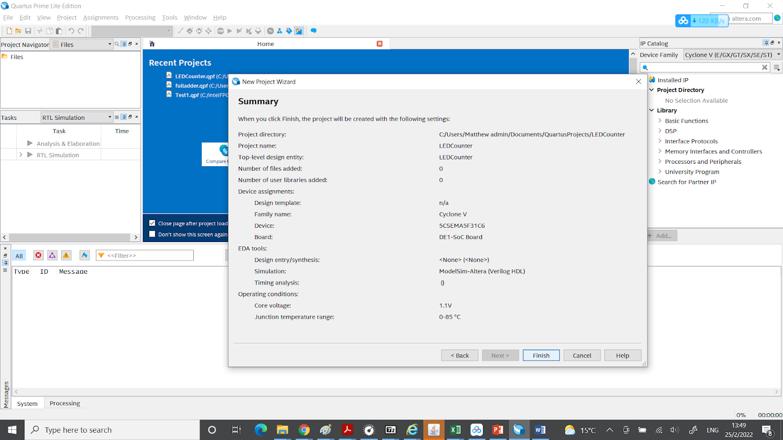
Either: 1) File à New Project Wizard or Click on the “New Project Wizard”
Name the project as (e.g.) "LEDCounter") as shown below:
Project Type: choose “Empty Project” and click “Next” à Add Files. Do not add any files and click Next.
Remember to choose "Modelsim-Altera" as the simulation tools.
Finish the New Project Wizard and a summary was shown below:
Specify the path of Modelsim-Altera:
Tools > Options > EDA Tools Options (e.g.) (pleases check the path of your installation)
Choose in Menu: File 🡪 New 🡪 Verilog HDL File
You can copy the Verilog codes below. Save it,and rename the Verilog file as LEDCounter.v
Verilog codes (of LED Counter):
// ***** ----- ----- ----- ----- ----- Code Starts Here ----- ----- ----- ----- ----- ***** //
module LEDCounter(
input clk,
input rstn,
input up_dnb,
output reg [3:0] count
);
reg [31:0] pre_count;
always @(posedge clk)
begin
if (rstn==0) begin
pre_count <= 31'b0;
end
else pre_count <= up_dnb ? (pre_count + 1'b1) : (pre_count - 1'b1);
//Assign 4 MSB to 4-bit output
count <= pre_count[31:28];
end
endmodule
// ***** ----- ----- ----- ----- ----- Code Ends Here ----- ----- ----- ----- ----- ***** //
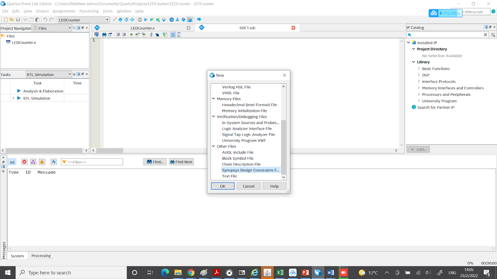
Create a New File. 🡪 Create a Synopsys Design Constraint File (.sdc) to define its clock:
Copy the codes and save it.
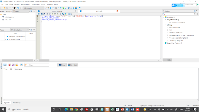
create_clock -name "clk" -period 20.000ns [get_ports {clk}]
derive_pll_clocks
derive_clock_uncertainty
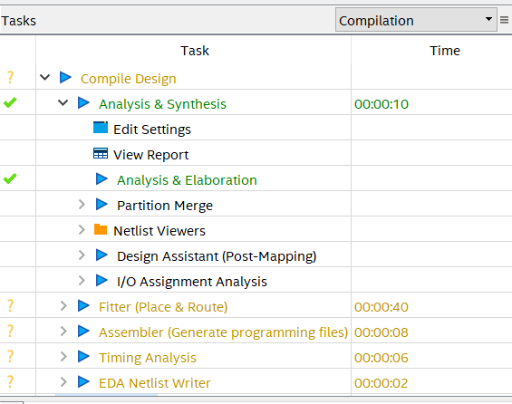
The period of the clock is 20 ns for the development board DE1-SOC which has built-in 50 MHz source (1/50MHz = 20 ns). You could compile the design and make sure that there are no errors:
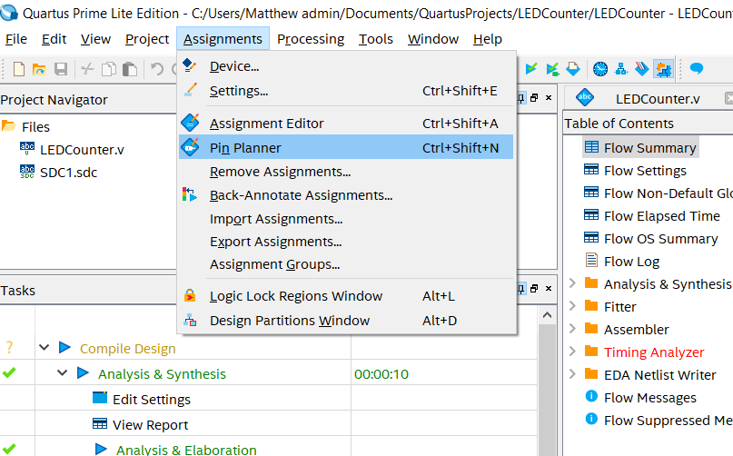
Assign the pin locations, by clicking "Assignments" => "Pin Planner":
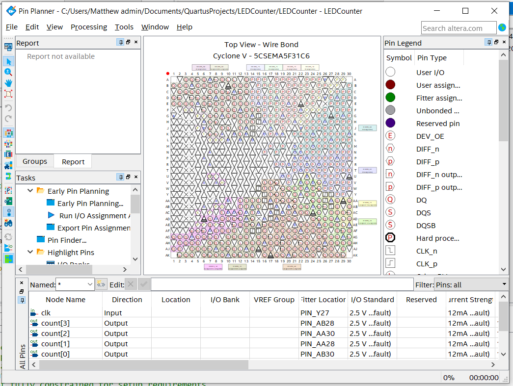
The "Pin Planner" was shown below:
With reference to the datasheet of the Terasic DE1-SOC, the assignments of the slide switches and push buttons and LEDs should be of the I/O pins.
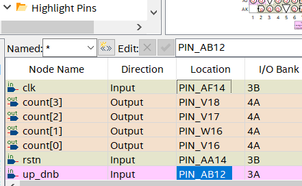
Assign the following pin “Location” to different I/Os of your FPGA design, as shown below:
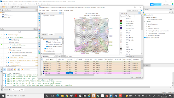
The assignments will be saved in the project file: “ledcounter.qsf”.
You can also copy the codes below and paste it in the ".qsf" file:
You can also copy the codes below and paste it in the ".qsf" file:
set_location_assignment PIN_V18 -to count[3]
set_location_assignment PIN_AF14 -to clk
set_location_assignment PIN_V17 -to count[2]
set_location_assignment PIN_W16 -to count[1]
set_location_assignment PIN_V16 -to count[0]
set_location_assignment PIN_AA14 -to rstn
set_location_assignment PIN_AB12 -to up_dnb
set_instance_assignment -name PARTITION_HIERARCHY root_partition -to | -section_id Top
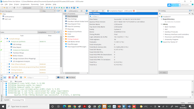
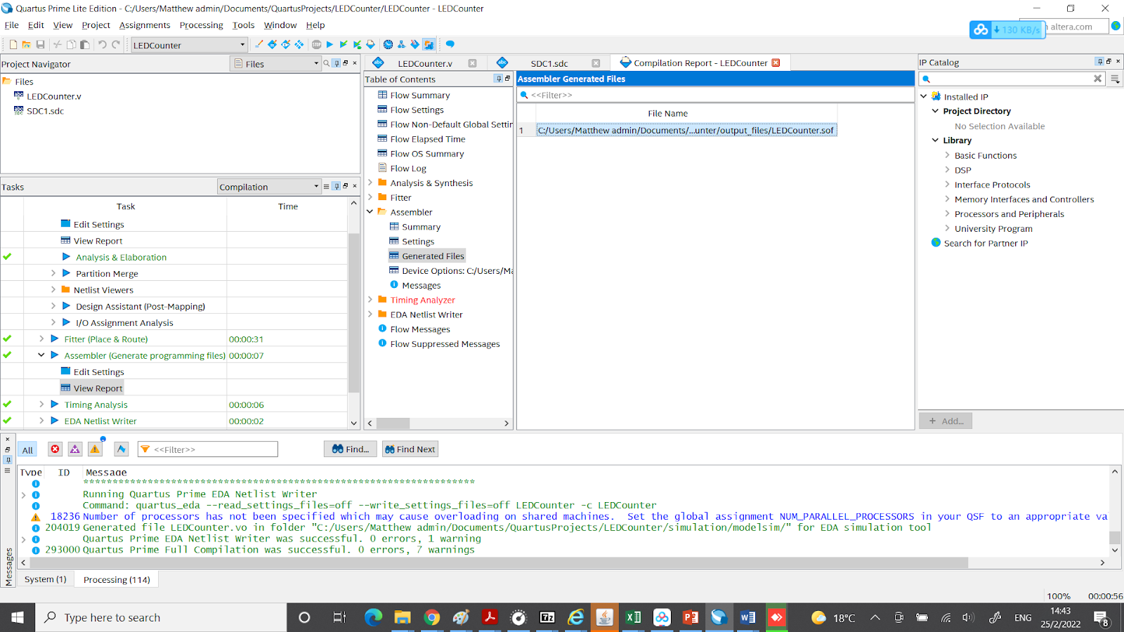
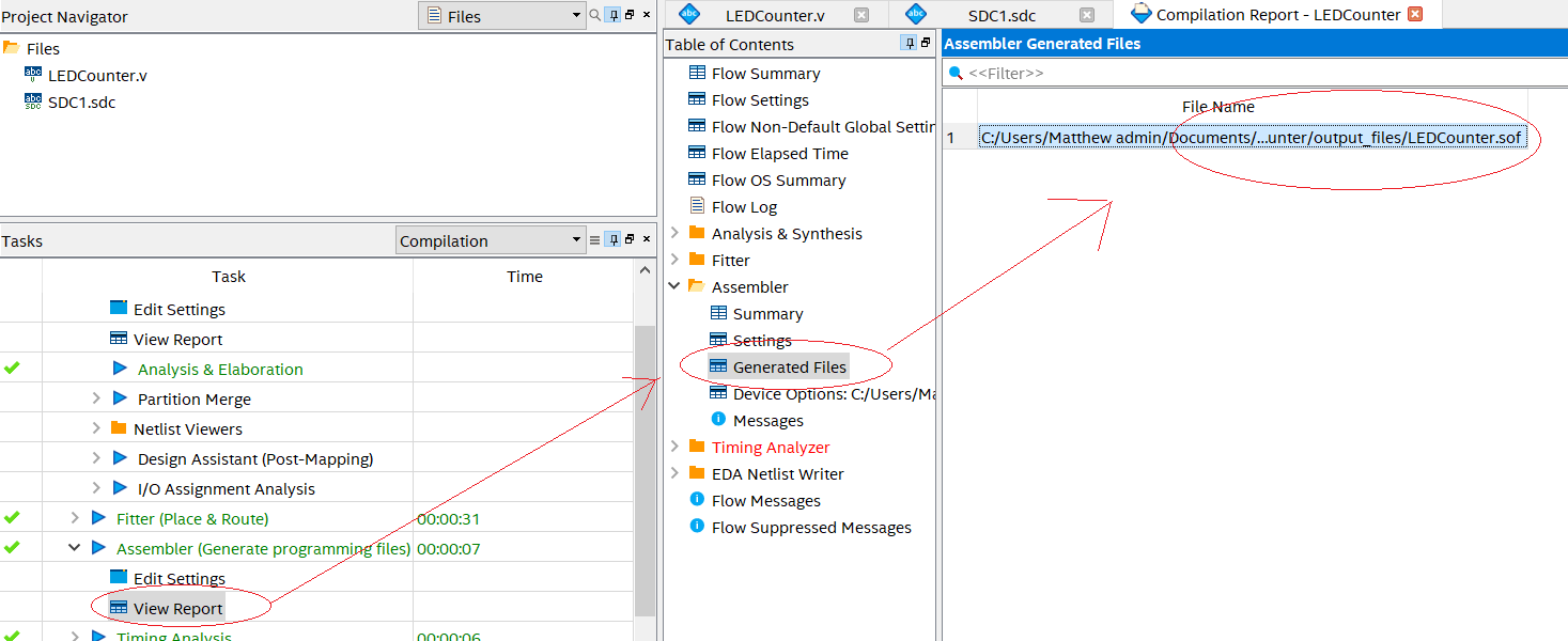
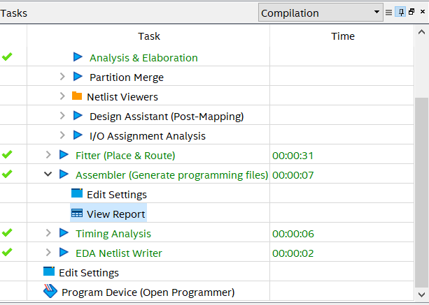
Recompile the project and generate a programming file (.\output\*.sof):
Click “View Report” and then click “Generated Files” to locate the programming file:
Connect the power adaptor to the FPGA development board DE1-SOC and connect the board to your PC, with the USB blaster cable. Remember to power on the board.
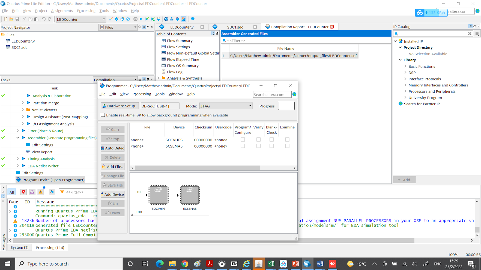
Open the FPGA programmer by clicking the “Program Device” under the window of “Tasks”:
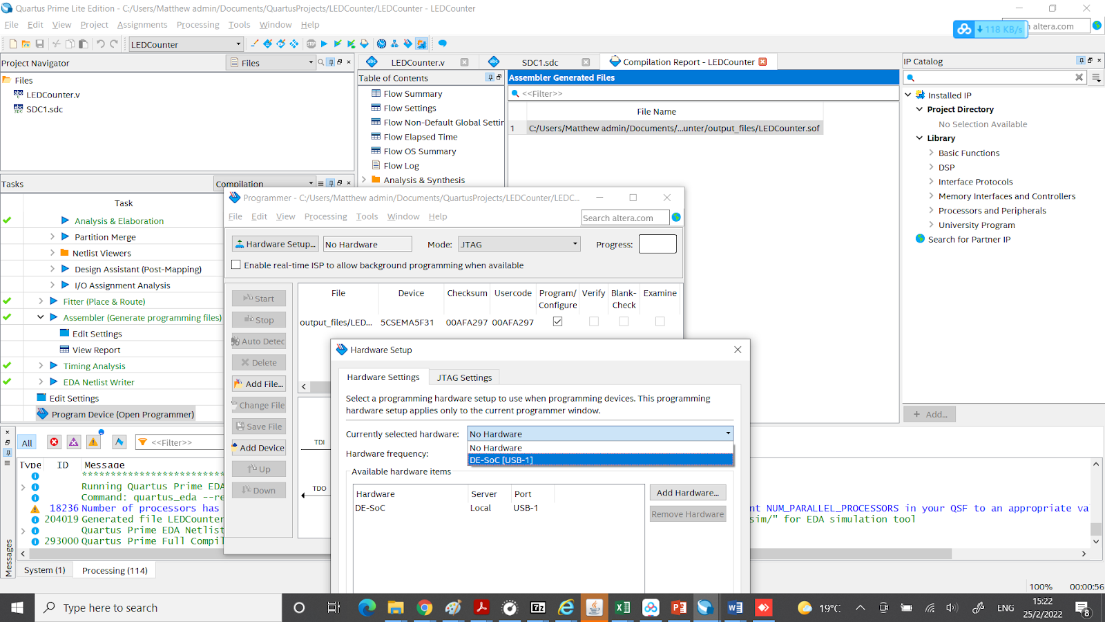
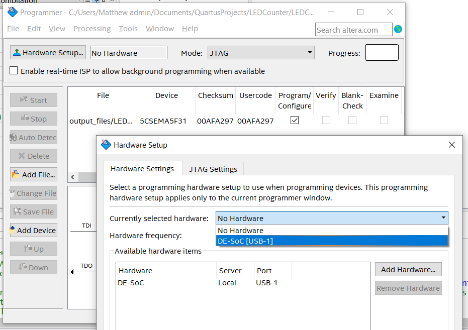
Click the button “Hardware Setup” and choose the development board “DE1-SOC”:
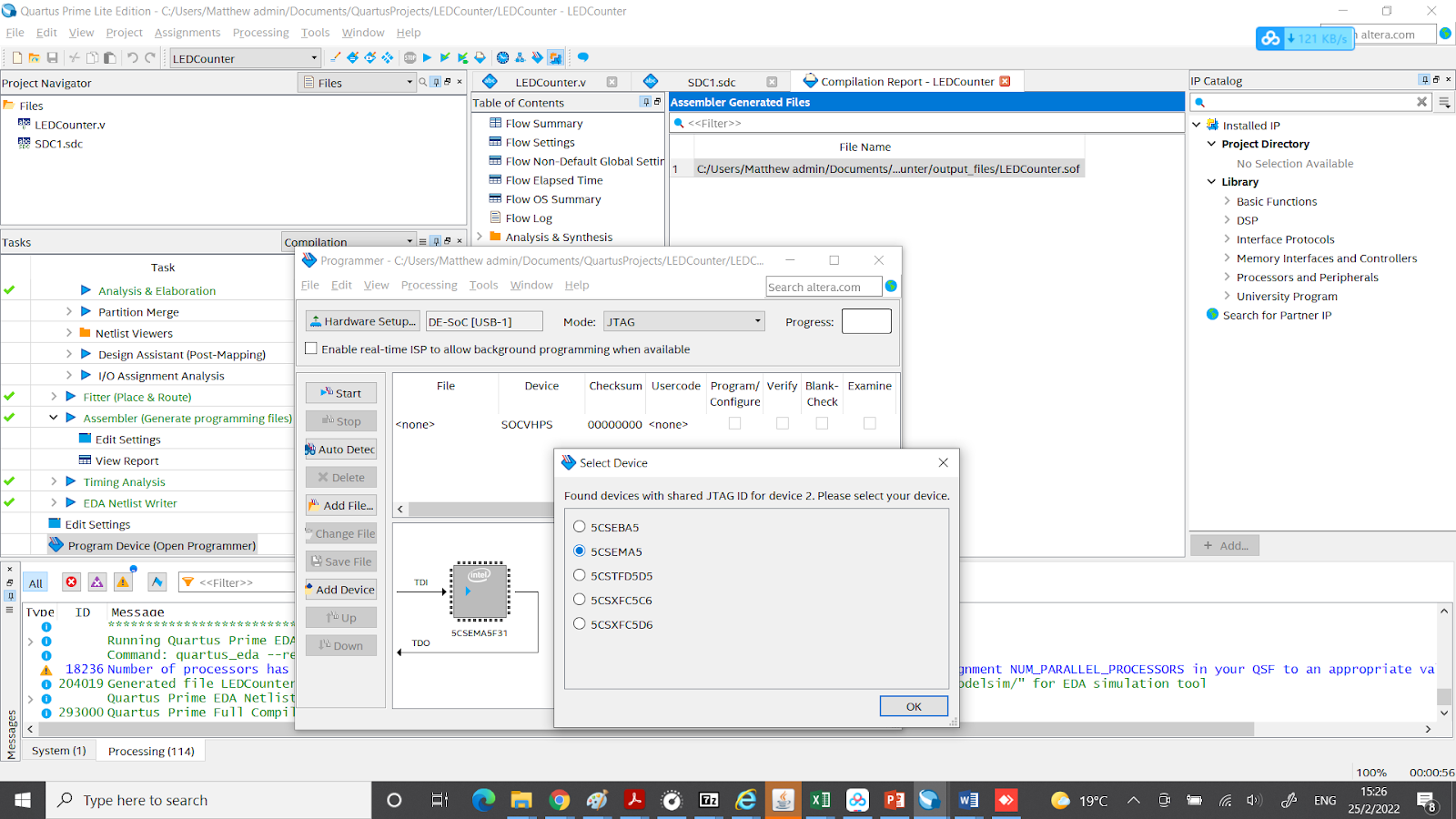
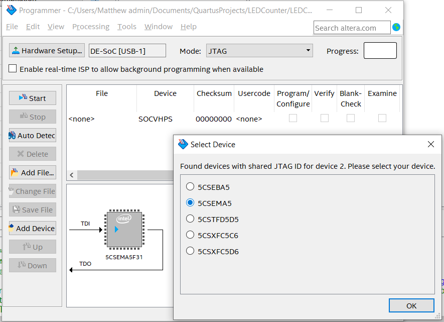
Click the button “Auto Detect” and choose the device “5CSEMA5”:
It should be as shown below.
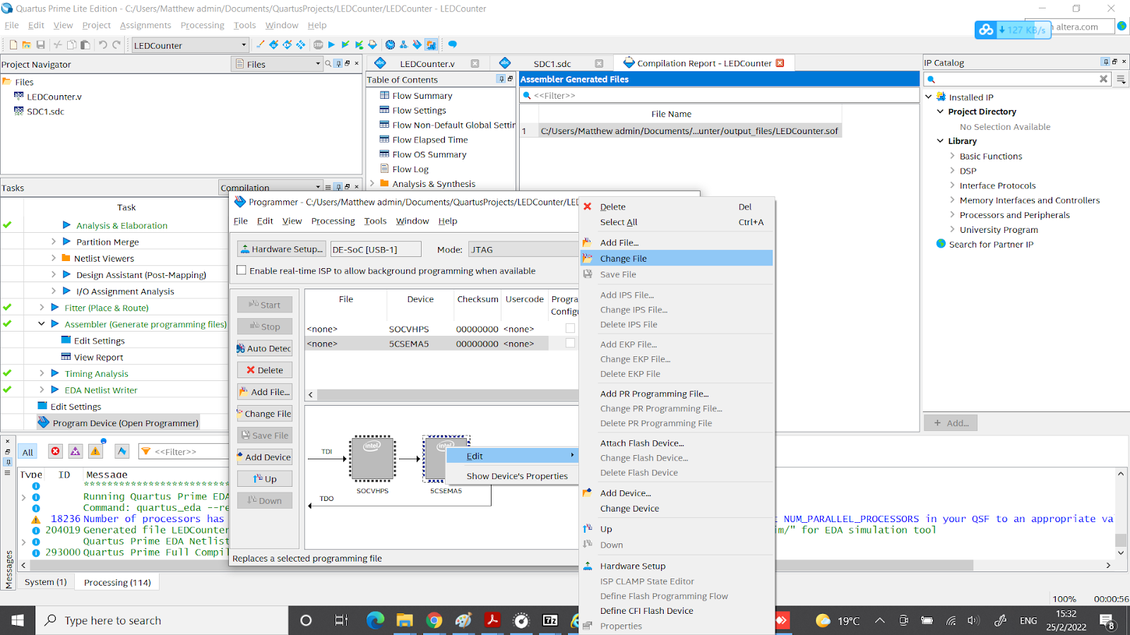
Right-click on the device 5CSEMA5 and select “Edit” 🡪 “Change File” and choose the sof file in the folder “out_files”:
Click the button “Auto Detect” to enable the “Start” button:
Click "Start" button to start the FPGA programming and if programming is successful, it will be as shown below (“Success” on the top right-hand corner at the programmer window):
You can see the LED counter to be running, with 4 LEDs
(32-bit counter, from 0000 🡪 0001 🡪 0010 🡪 0011 🡪 0100 🡪 0101 🡪 ….. 🡪 1101 🡪 1110 🡪 1111 🡪 0000 🡪 0001 🡪 …..
“0” is LED off and “1” is LED ON.
Demonstration video: https://youtu.be/P39Ay-hOoOM
(Troubleshooting: some students failed to have the LED demo, just because they failed to assign the pin locations of the I/O cells (Pin Planner))
-----
Testbench Example: (Text below and picture using Verilog text editor (e.g.
Notepad++)
// *****************************************************************************
// This file contains a Verilog test bench template that is freely editable to
// suit user's needs .Comments are provided in each section to help the user
// fill out necessary details.
// *****************************************************************************
// Generated on "02/22/2024 20:37:58"
// Verilog Test Bench template for design : LEDCounter
//
// Simulation tool : ModelSim-Altera (Verilog)
//
`timescale 1 ps/ 1 ps
module LEDCounter_vlg_tst();
// constants
// general purpose registers
reg eachvec;
// test vector input registers
reg clk;
reg rstn;
reg up_dnb;
// wires
wire [3:0] count;
// assign statements (if any)
LEDCounter i1 (
// port map - connection between master ports and signals/registers
.clk(clk),
.count(count),
.rstn(rstn),
.up_dnb(up_dnb)
);
initial begin
clk = 0;
forever #20 clk = ~clk;
end
initial
begin
// code that executes only once
// insert code here --> begin
rstn=0;
up_dnb = 0;
#200;
rstn=1;
// --> end
$display("Running testbench");
end
always
// optional sensitivity list
// @(event1 or event2 or .... eventn)
begin
// code executes for every event on sensitivity list
// insert code here --> begin
@eachvec;
// --> end
end
endmodule
// ----- ----- ----- //
Simulation results: (ModelSIm)
Electronic Component Purchases:


留言
張貼留言